Memory and RAM
This is the second entry on my series on computer fundamentals. In the previous post we talked about bits, codes and logic gates. These are the fundamental building blocks for the 2 main elements that make up a computer, the Random Access Memory (RAM) and the Central Processing Unit (CPU). These 2 pieces work in tandem to store and process all the instructions and data that allow computers to do the things they do. In todays entry we’ll explore the RAM and its main components, the memory registers. But before we get to that we’ll talk about sequential logic and it’s importance on highly synchronized systems such as computers.
Sequential logic and the memory bit
Contrary to the chips we’ve seen so far sequential chips have a dependency on time in addition to their regular inputs. The passage of time in a computer is tracked by a special chip known as clock which broadcasts an oscillating signal to all sequential chips in the system letting them know when a unit of time has passed. We could implement a simple version of a clock like this:

We can see how the clock output will continuously oscillate between 1 (“tick”) and 0 (“tock”). The time elapsed between the beginning of a tick and the end of a tock is known as a clock cycle and corresponds to a discrete unit of time. Sequential chips can then listen to this “passage of time” and account for it when calculating their output.
The first task in our quest to understand the RAM is to build a memory bit, basically a chip that can remember the state of one bit which has been set at some point in the past. We are going to based our design on a sequential chip known as D flip flop, which we will be treating as a black box. Feel free to check its NAND gate based implementation on the link I provided.

The flip flop’s output at any given time t is simply its historical input at the previous period of time t-1 so in essence the flip flop just outputs a delayed signal. We are interested in building a memory bit that can hold onto a value potentially forever so a mere flip flop won’t do because the output value gets overridden after each cycle. We can achieve ‘true’ memory by extending the flip flop functionality using the multiplexer gate derived on my previous post:

In the diagram above we have a MUX gate with 3 inputs load, in and out, notice how the latter is fed back into the bit from the DFF output. The load bit will determine whether or not we override out with the incoming in signal. We can wire these devices in such a way that load = 1 lets in through overriding out on the next cycle, and load = 0 feeds back out into the DFF again perpetuating its value onto the next cycle.
We can better understand this by examining example presented on the table above. Let’s say we want to store the value 1 on this particular memory bit which is currently set to 0. We start at time = 0 by setting load and in to 1 allowing in to reach the DFF. At time = 1 in replaces out and our memory bit starts emitting the value 1, at this point we also turn set load = 0 to prevent the information on the DFF from being overwritten by future incoming in. At subsequent time cycles the memory bit will keep outputting 1 as long as we do not flip load back on, effectively remembering the information for as long as we need to.
Why sequential logic matters
We could make the case that we do not need a time-delay to be able to remember an output. We could for example achieve the same result just by using a multiplexer that feeds its output back to itself like we see in the following diagram:

On the surface this device behaves similarly to the memory bit we described above: when load = 1 we override out with in, and with load = 0 we perpetuate out. Now this implementation has some issues the first one being related with systems that loop on themselves like we see below:

This diagram shows a NAND chip that operates on the output of our bogus memory bit Y, and a constant bit X with the value of 1. The output of the NAND gate then feeds back into our memory bit. The issue here has to do with the value of out. Imagine that initially the values of X and Y were 1 and 0 respectively, after the first iteration the resulting value of out will be 1. On the second iteration though, we’ll have X = 1 and Y = 1 which will produce out = 0 which will again change the value of X and and so on.
So because our bogus memory bit X chip is oblivious to the notion of time the value of out has effectively become a function of itself and will never stabilized. The time delay introduced by the sequential memory bit prevents this from happening because X will no longer change immediately with out letting the system stabilized to the correct output, after every iteration of the system.
The second issue has to do with synchronization to better understand it we have to look at the situation presented on the diagram below:

In the diagram above we have again a NAND gate operating on two bits X and Y. In this case X is very close to the NAND gate and Y very far. The output of the NAND in gate then feeds into our bogus memory bit and its then broadcast to another mission critical part of the system.
The problem here is the difference in proximity of X, and Y to the NAND gate. While electricity runs very fast through the bit wires it is also bound to natural physical constrains. This means that X will get to the NAND gate long before Y does. So for a considerable period of time and until Y reaches the gate the value of in and thus out will not be correct. But because our bogus bit provides not time delay it will immediately broadcast the incorrect result to the rest of the system, which is not desirable.
How would the sequential bit help in this case? Let’s add a DFF to our previous diagram and see what happens
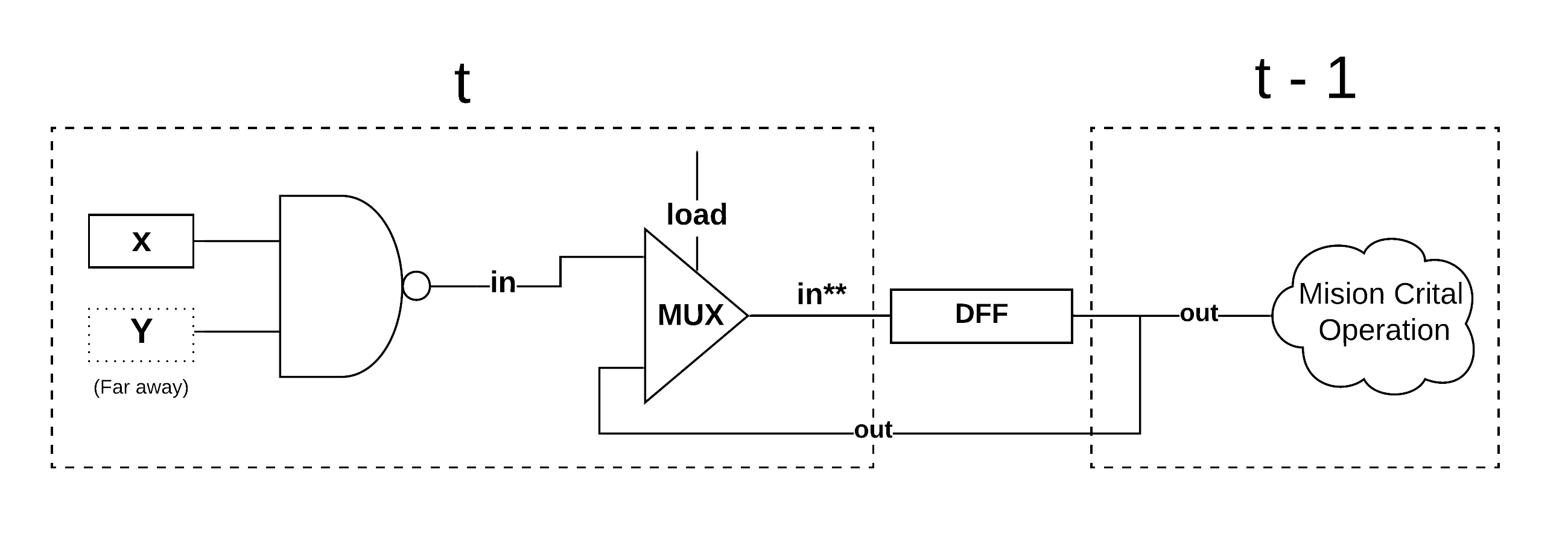
As I explained before the DFF outputs a delay signal which means that the current out was the historical in** right at end of the clock cycle t - 1 so everything enclosed within the dotted box on the right is guaranteed to be on steady state and correct as long as the clock cycle is sufficiently long to allow Y reach the NAND gate. Also since out is now locked at the in**t-1 we prevent the runaway value situation explained on the first scenario where out never stabilizes.
I hope this helped demonstrate the importance of the clock along with the sequential logic when coordinating logical circuits. From now on we will be treating the memory bits as black boxes to simplify the upcoming diagrams.
Registers and Buses
We already understand how a memory bit works but as we discussed before on the previous entry the amount of information that we can encode on single bit is very limited. So generally computers stack several of these memory bits to store more meaningful patterns. A set of memory bits holding a particular sequence is known as a register. The amount of memory bits on each register will generally depend on the cpu architecture, 16 bit processors will have 16 bits registers, 32 bit processors 32 bits registers and so on. We can see a representation of a register with n bits of memory in the diagram below. The memory bits have been abstracted away into the Bit[] boxes but they keep the same api (inputs: in, load, outputs: out) derived on the previous section.

Notice how each individual bit has it’s own in and out but they all share the same load bit. So while every bit in a register it’s independent (they each have their own wire) they all get set (load = 1) or locked (load = 0) at the same time. This is because each register is meant to be a self contained, discrete unit of information and we normally just want to store a single concept in them like a letter, a number, an instructions etc. So generally when we override a register we fully replace its content with new information as opposed to tweak every bit individually. This fact opens an interesting discussion about how the information flows across the computer.
The CPU needs to have access to any register at all times and it also needs to be able to freely move data from and into any of them. For this to happen there needs to be some wiring in place that allows any register to reach (almost) any part of the computer, such wiring is known as bus or data bus. The bus consists of parallel wires (bits) that will go across the whole computer. The bus width naturally matches that of the registers since that’s the size of the data it will be transporting. The diagram above shows the bus wires coming in and out of the registers to carry the information forward.
Now that I’ve explained what registers are I’ll be simplifying their representation on future diagrams. Also, bus wiring will be represented as a double line. Lastly, in some cases we’ll also encounter wiring of arbitrary size for those I’ll be using an array notation like [0..1] to denote their width.
RAM
The RAM is composed of many registers carefully ordered in a grid like structure and it’s the physical location where most of the actively running programs and data is stored. The great thing about RAM is that, regardless of size, we can access any of its registers at equal speed without paying any time penalty thus, the name “Random Access Memory”. The top level api for the RAM could look like this:

This RAM chip has 3 inputs, a register address, an incoming payload in and a load bit. The output out consists of a specific register output. At any point in time the RAM can only store and/or retrieve the information for one particular register. In order to select such register the CPU needs to provide that specific register’s location or address within the RAM. The RAM can then parse the address and use it to route the load bit to the particular register the CPU is interested on activating. Lastly, on the way out the RAM uses the address again to ensure that the information emitted to the rest of the system is that of the register the CPU is requesting an no other.
It is no coincidence that the RAM api closely resembles that of its registers (in, load, out), after all registers are the underlying source of information. But the RAM also requires some extra circuitry to be able to parse the address and route the load to the targeted register and then to decide which registry info gets to become out. We can take care of the incoming load bit by using a demultiplexer as shown below:

This de-multiplexer takes the load bit and routes it to load0 or load1 depending of the address passed in. In this case when address = 0 the load gets passed to load0 which would then get fed to the register located at 0, and when address = 1 load will propagate through load1 which will get fed to the registers located at 1, respectively. On the output side we can use a multiplexer to ensure we’re emitting the information of the correct register.

This particular MUX propagates the information stored on the register at position 0 out0 or 1 out1 depending on the address passed in. If address = 0 out0 and vice versa.
Now it’s silly to think that a RAM chip will only have 2 locations 0 and 1 so these DMUX and MUX implementations are a bit limiting. In reality they are usually extended to a multi-way configuration which allows them to parse and redirect information to longer addresses. We can see the 4-way implementations of these gates below:

We have increased the address size by 1 digit effectively doubling the possible locations to 4 (00, 01, 10, 11) but this can be hypothetically extended to any address size our computer architecture supports. At this point we have all the building blocks required to build the RAM all we need to do is to put them together.

Notice how in gets fed to every register at the same time, this is ok because as we’ve discussed extensively by now the DMUX will ensure that only 1 register will be activated and potentially overwritten by the incoming payload in. The same thing with their outputs, the MUX will make sure that only the targeted register propagates its info to out.
Another way to expand the amount of memory is by stacking several RAM chips together, as we can see in the diagram below:

All we’ve done in the case is to break down the 4 digits address into 2 parts. The first 2 digits are fed into a top level DMUX to see which RAM gets to process the incoming load, and then we feed the last 2 address digits to all RAM chips. This will ensure that only one register within a particular RAM will ever be active, which is exactly what we need. Yet again you can imagine we can keep extending this concept till we reach the RAM capacity we want.
Thanks for reading!